Korean media reports that Samsung Electronics Exynos Mobile Application Processor (AP) development strategy will undergo major changes within three years, and Samsung has decided to ease the 2027 1.4 nanometer production plan. According to ZDNet Kor...

Korean media reports that Samsung Electronics Exynos Mobile Application Processor (AP) development strategy will undergo major changes within three years, and Samsung has decided to ease the 2027 1.4 nanometer production plan.
According to ZDNet Korea, Exynos chips are Samsung's own mobile AP and have always been the first application product for its cutting-edge process technology in the wafer factory. This makes its development route diagram closely related to the process process of the wafer factory, and is extremely sensitive to any technological route changes. Therefore, under the new strategic direction, industry analysis believes that when Samsung Electronic Systems LSI Business Department develops the next generation of mobile APs, it will focus its main research and development and optimization on a mature 2nm process. This means that Samsung is carefully considering its future technical pace.
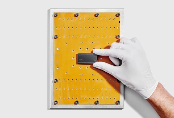
Mobile AP is the core brain of modern smartphones and other IT equipment, and also integrates a variety of high-performance semiconductor components such as central processors (CPUs), graphics processors (GPUs), and memory. For a long time, Samsung Electronics has continuously developed and optimized its own Exynos series of mobile AP products through its system LSI business department, which is specialized in system semiconductor design. The final output of these Exynos chips is fully responsible for Samsung's crystalline industry.
Samsung plans to produce the first generation of 2 nanometers (SF2)-based Exynos 2600 chips in the second half of the year. This is a new generation of flagship chips that are expected to be used as a core processor and will be launched in the Galaxy S26 series of smart phones in the first season of 2026. In addition, the System LSI Business Department has begun to conceive of developing blueprints for the next generation of AP products, and will follow the process route diagram of Samsung Cylinder Factory, and is expected to further adopt the second generation 2nm (SF2P) process in 2026.
However, in the face of the development of the next generation of AP products, Samsung's strategy adjustment is more urgent and necessary. Although the Samsung Glass OEM business was originally planned to push the 1.4 nanometer process (SF1.4) to commercial production around 2027. However, in the recent development of the most advanced wafer wafer process, we have encountered significant technical difficulties, which directly led to the delay of the 1.4-nanometer production plan. Marketers predict that the production time of this key process will also be pushed to 2028-2029 as soon as possible.
Samsung has sent clear messages to its major customers and partners through the "SAFE (Samsung Advanced Foundry Ecosystem) Forum 2025" held in the United States earlier this month, which is to increase the development of next-generation processes, and the company will invest more first and concentratedly in resources to stabilize the existing 2-nanometer and 4-nanometer processes and continuously improve its production yield.
According to the Shenzhen-based semiconductor industry, there is a high degree of mutual connection between the mobile AP development plan of Samsung system LSI and the long-term process route diagram of Samsung crystalline plants. Therefore, the current decision by Samsung's crystalline mill to focus on the improvement and upgrading of the 2nm process also means that future Exynos series chips will have to continue to rely on and use 2nm process technology in the medium and long term.
Even though Samsung plans to launch new 2nm process technologies such as SF2A and SF2Z in 2027, the application targets of these advanced processes do not include mobile processors. Specifically, the SF2A process is mainly locked in the automotive semiconductor market, while the SF2Z process is designed for server and high-performance computing (HPC) fields. Especially SF2Z, which will integrate advanced BSPDN (backside power supply) technology. However, considering the high sensitivity of mobile AP to cost, applying complex and costly BSPDN technology to mobile processor products is currently not economically beneficial and feasible.
Another market insider pointed out that the current market price of smart phones has been difficult to increase significantly, but the production costs of cutting-edge wafer-machinery processes are rising rapidly. This effect should enable strategies that single-purpose improvements in mobile processor performance have gradually reached the upper limit of development. In this regard, from the perspective of medium-term market competition, can Samsung successfully implement DTCO (co-optimization of design technology) in the 2nm process, making the highest degree of coherence and optimization between semiconductor design and its manufacturing technology. It is particularly important to improve product performance, reduce costs and shorten development cycles in cutting-edge processing areas with relatively low technological maturity.