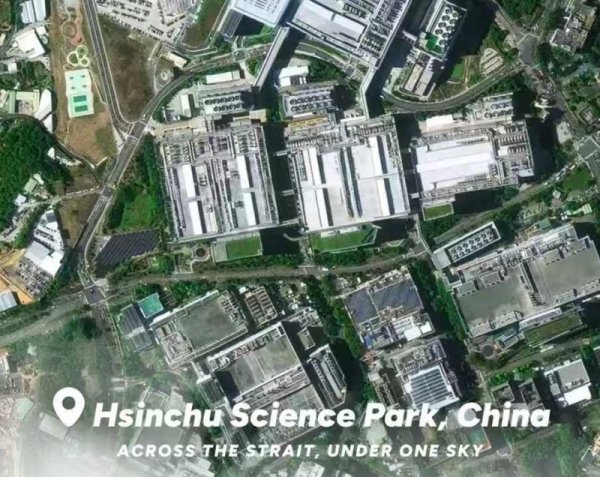
As the AI wave drives the global semiconductor industry, wafer foundry is entering the new era of Foundry 2.0. A highly integrated supply chain composed of wafer foundries, IDMs, and packaging and testing companies is gradually taking shape. Resea...
As the AI wave drives the global semiconductor industry, wafer foundry is entering the new era of Foundry 2.0. A highly integrated supply chain composed of wafer foundries, IDMs, and packaging and testing companies is gradually taking shape. Research firm Counterpoint pointed out that the strong growth in demand for AI computing and flagship smartphones has promoted the simultaneous upgrade of advanced manufacturing processes and packaging, driving the industry towards a higher profit structure.
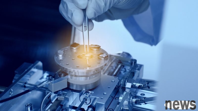
According to the latest report from Counterpoint Research, 3nm and 4/5nm processes continued to be in short supply in the third quarter, mainly driven by AI accelerators and high-end mobile phones; demand for advanced packaging also remained strong, and CoWoS and SoIC technologies became the focus of the market. In contrast, demand for mid-level and mature processes has slowed slightly, with utilization rates falling back to 75% to 80%.
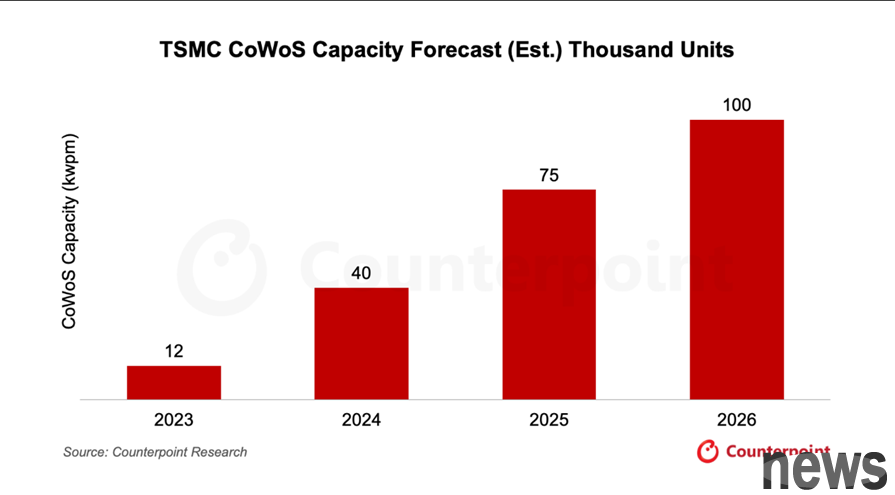
In the wafer foundry sector, TSMC continues to lead the way, with revenue reaching US$33.1 billion in the third quarter of 2025, higher than the company's original expectations. At the same time, TSMC is also actively expanding its CoWoS-L production capacity, which is expected to reach 100,000 wafers per month by the end of 2026 to support the needs of NVIDIA GPUs and AI accelerators such as Google, AWS, and Meta.
As for Samsung and Intel, they continue to promote the Foundry 2.0 strategy, but they are still in the development stage in terms of expanding their customer base. Intel's 18A process has been introduced to the Panther Lake platform, and customer foundry services will be launched in 2026, and will be adjusted to a "customer commitment-oriented" production capacity strategy to ensure that production expansion is closely linked to actual demand; Samsung Electronics' advanced process utilization rate continues to increase, with 2nm wafer shipment growth as the main driving force. Future performance will depend on the stability of 2nm technology and the results of cooperation with Tesla, thereby consolidating the high-end process layout.
Packaging giant ASE’s revenue in the third quarter is estimated to reach US$5 billion, a year-on-year increase of 9%, mainly due to TSMC’s CoWoS-S overflow orders and AI, high-end mobile packaging demand, and the adoption of 2.5D and 3D packaging technologies in AI accelerators and smartphone SoCs, thus continuing to grow.
William Li, senior analyst at Counterpoint Research, said that the third quarter of 2025 is an important milestone for the global foundry industry to move towards Foundry 2.0. As the demand for AI and high-performance computing (HPC) continues to be strong, the development of advanced processes and packaging will be deeply integrated, driving a new wave of semiconductor innovation in data centers, consumer electronics and smart systems.
Further reading: Evidence has been obtained! China controls US to launch cyber attack and invades its national time service center Bloomberg: U.S. Department of Commerce withdraws Arrow Electronics affiliates from U.S. blacklist